Clock Distribution
Clock distribution is as shown in Figure 7.
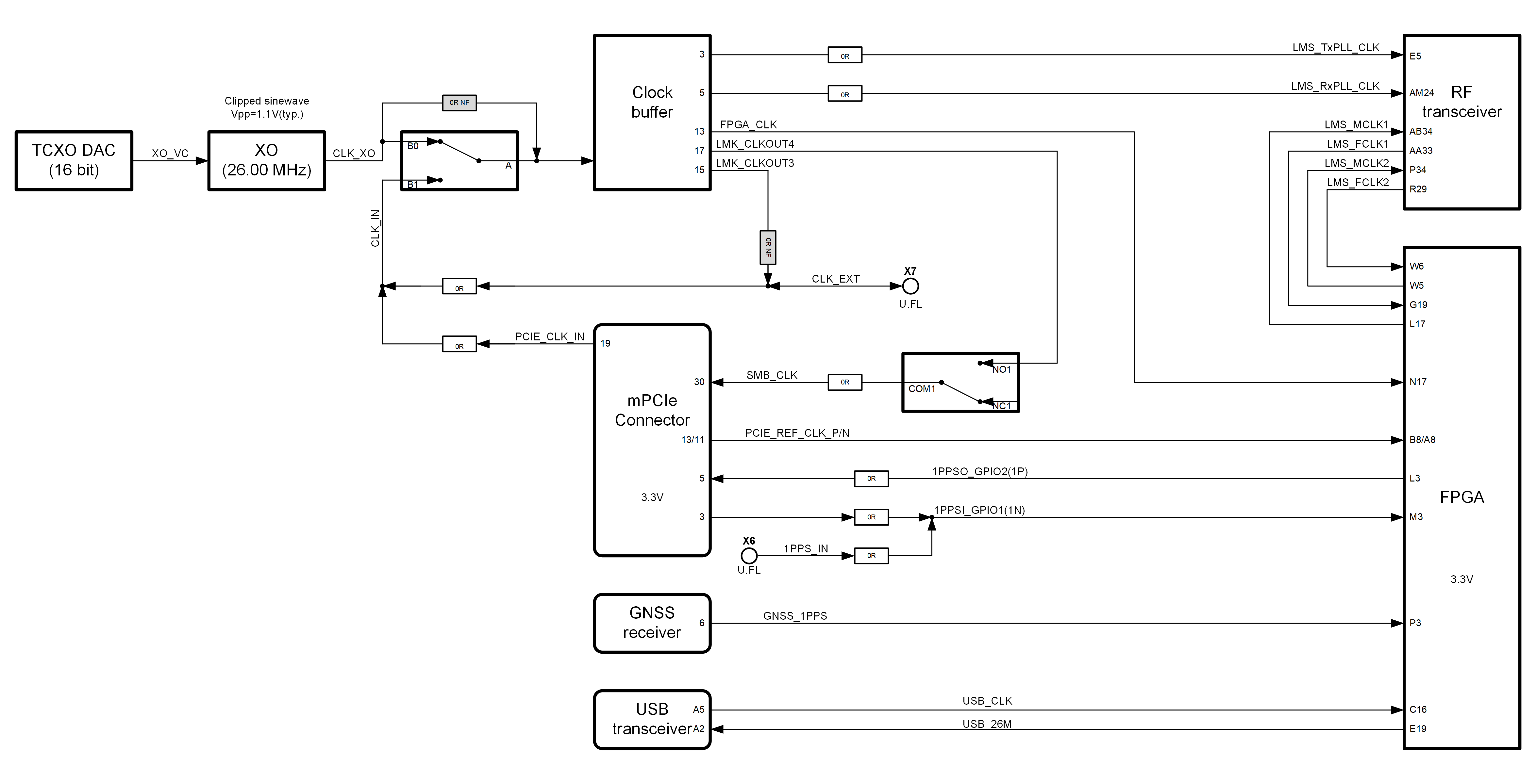
Figure 7. LimeSDR XTRX v1.3 board clock distribution block diagram
LimeSDR XTRX board features an on board 26.00 MHz VCTCXO as the reference clock for LMS7002M RF transceiver and FPGA PLLs.
Rakon E6982LF 26.00 MHz voltage controlled temperature compensated crystal oscillator (VCTCXO) is the clock source for the board. VCTCXO frequency may be tuned by using 16 bit DAC (IC17). Main VCTCXO parameters are listed in Table 5.
Frequency parameter |
Value |
|---|---|
Calibration (25°C ± 1°C) |
± 1 ppm max |
Stability (-40 to 85 °C) |
± 0.2 max |
Long term stability (1 year, 3 years) |
± 1 ppm max, ± 2 ppm max |
Control voltage range |
0.5V .. 2.8V |
Frequency tuning |
± 3 ppm |
Slope |
+4 ppm/V |
Analogue switch gives option to select clock source for RF transceiver and FPGA from buffered VCTCXO onboard clock XO1 (CLK_XO) and external U.FL (X7)/mPCIe (X10) sources (CLK_IN). Buffered VCXO clock (LMK_CLKOUT3 and LMK_CLKOUT4) can also be fed to other board using U.FL (X7)/mPCIe (X10)connectors.
The board clock lines and other related signals/information are listed in Table 6.
Schematic signal name |
Source |
Destination |
I/O standard |
|---|---|---|---|
CLK_XO |
(VC)TCXO (XO1) |
Analog mux |
Clipped sinewave |
CLK_IN |
CLK_EXT or PCIE_CLK_IN |
Analog mux |
3.3V |
CLK_EXT |
U.FL connector |
CLK_IN |
3.3V |
PCIE_CLK_IN |
mPCIe connector |
CLK_IN |
3.3V |
LMS_TxPLL_CLK |
Analog mux |
RF transceiver |
1.8V |
LMS_RxPLL_CLK |
Analog mux |
RF transceiver |
1.8V |
FPGA_CLK |
Analog mux |
FPGA |
3.3V |
LMK_CLKOUT3 |
Analog mux |
External |
3.3V |
LMK_CLKOUT4 |
Analog mux |
External |
3.3V |
LMS_MCLK1 |
RF transceiver |
FPGA |
3.3V |
LMS_FCLK1 |
FPGA |
RF transceiver |
3.3V |
LMS_MCLK2 |
RF transceiver |
FPGA |
3.3V |
LMS_FCLK2 |
FPGA |
RF transceiver |
3.3V |
PCIE_REF_CLK_P/N |
PCIe |
FPGA |
3.3V |
1PPSO_GPIO2(1P) |
FPGA |
mPCIe |
3.3V |
1PPSI_GPIO1(1N) |
External |
FPGA |
3.3V |
1PPS_IN |
External |
FPGA |
3.3V |
GNSS_1PPS |
GNSS |
FPGA |
3.3V |