RF Network Control
LimeSDR XTRX RF network contains matching networks, RF switches and U.FL connectors (X1, X3 - TX and X2, X4 - RX) as shown in Figure 6.
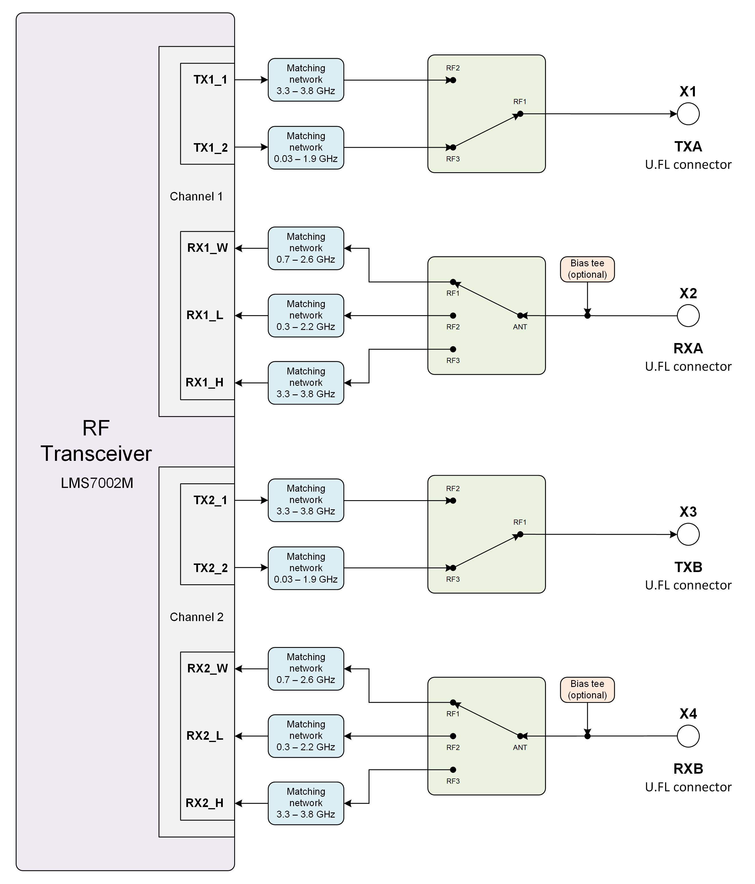
Figure 6. LimeSDR XTRX v1.2 RF diagram
LMS7002M RF transceiver TX and RX ports has dedicated matching network which determines the working frequency range. More detailed information on LMS7002M RF transceiver ports and matching network frequency ranges is listed in the Table 3.
LMS7002M RF transceiver port |
Frequency range |
|---|---|
TX1_1, TX2_1 |
3.3 GHz – 3.8 GHz |
TX1_2, TX2_2 |
30 MHz – 1.9 GHz |
RX1_H, RX2_H |
3.3 GHz – 3.8 GHz |
RX1_W, RX2_W |
700 MHz – 2.6 GHz |
RX1_L, RX2_L |
300 MHz – 2.2 GHz |
RF network switches are controlled via 2.4V logic signals. This is achieved by resistor dividers connected between FPGA (TX_SW, RX_SW1, RX_SW2) and switch control pin (TX_SW_DIV, RX_SW1_DIV, RX_SW2_DIV). RF network control signals are described in the Table 4.
Component |
Schematic signal name |
I/O standard |
FPGA pin |
Description |
|---|---|---|---|---|
SKY13330-397LF(IC5 and IC6) |
TX_SW/TX_SW_DIV |
3.3V |
P1 |
FPGA 3.3V logic level signal divided to 2.4V logic level. |
SKY13414-485LF(IC3 and IC4) |
RX_SW1/RX_SW1_DIV |
3.3V |
K3 |
FPGA 3.3V logic level signal divided to 2.4V logic level. |
RX_SW2/RX_SW2_DIV |
3.3V |
J3 |
FPGA 3.3V logic level signal divided to 2.4V logic level. |